Finally got my SN74LV8153 chips. Did some coding in the background, but without this chip, it wasn’t value added to mess with it. Mouser is 20 or 30 miles away. They couldn’t verify my credit card, so I had to just wait on DigiKey.
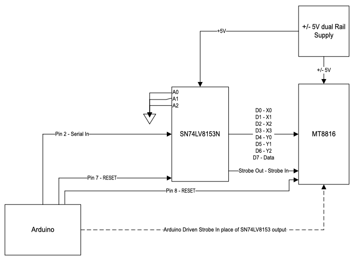
I wired it all up. The SN74LV8153 has 8 parallel outputs. The crosspoint has 7 input address bits plus the function. it all adds up:
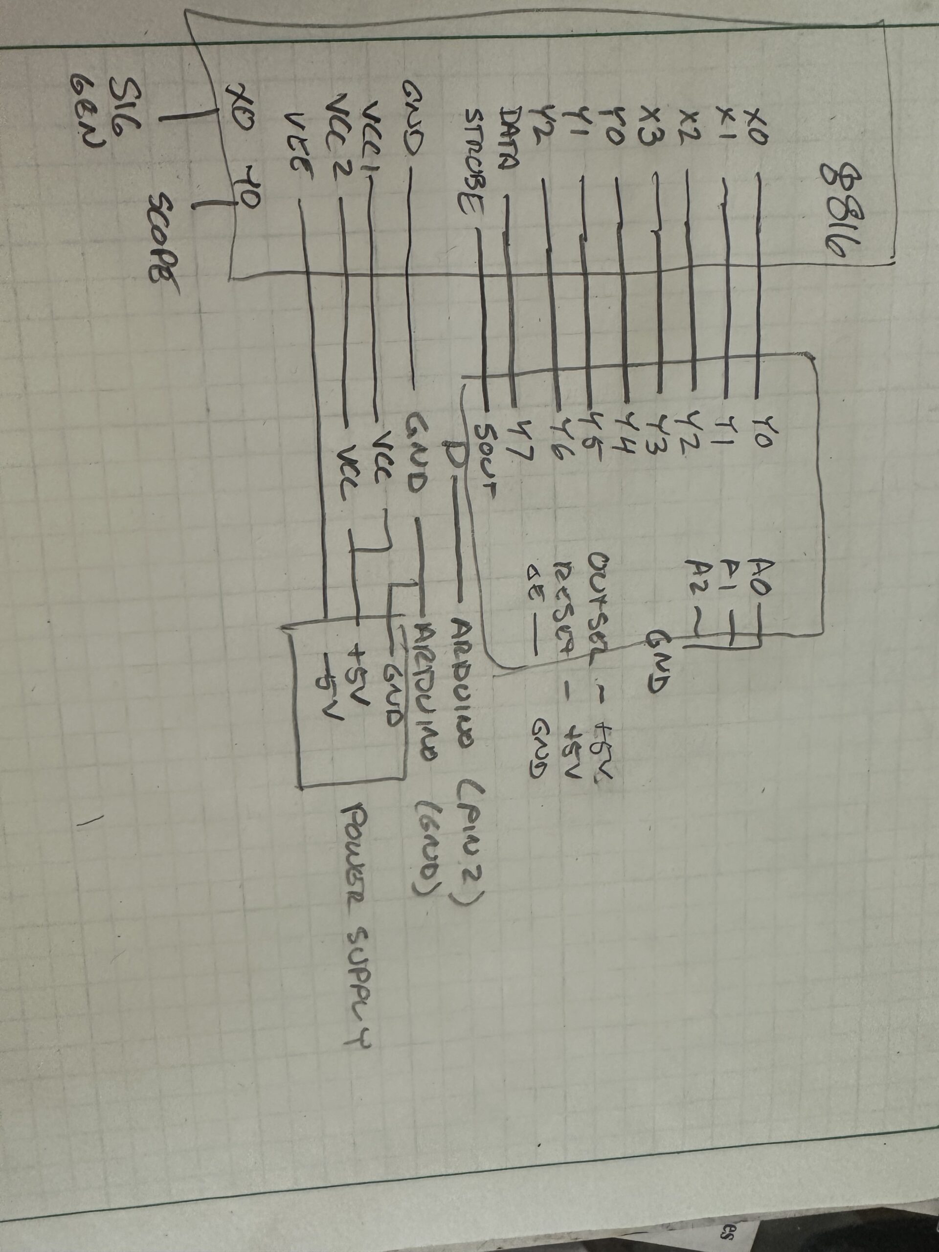
The SOUT on the SN provides a negative going pulse that seems to work fine for triggering the STROBE line on the 8816.
You can see how DATA on the 8816 (turning a specific switch on or off) is wired to Y7 on the SN chip. Within my code, I roll the switch addresses and function into a single 8-bit control word, which is then decoded, and sent bit by bit to the serial port in the format the SN needs it (I opted to manually bit-bang a pin, rather than use the on-board UARTs, which might be needed elsewhere).
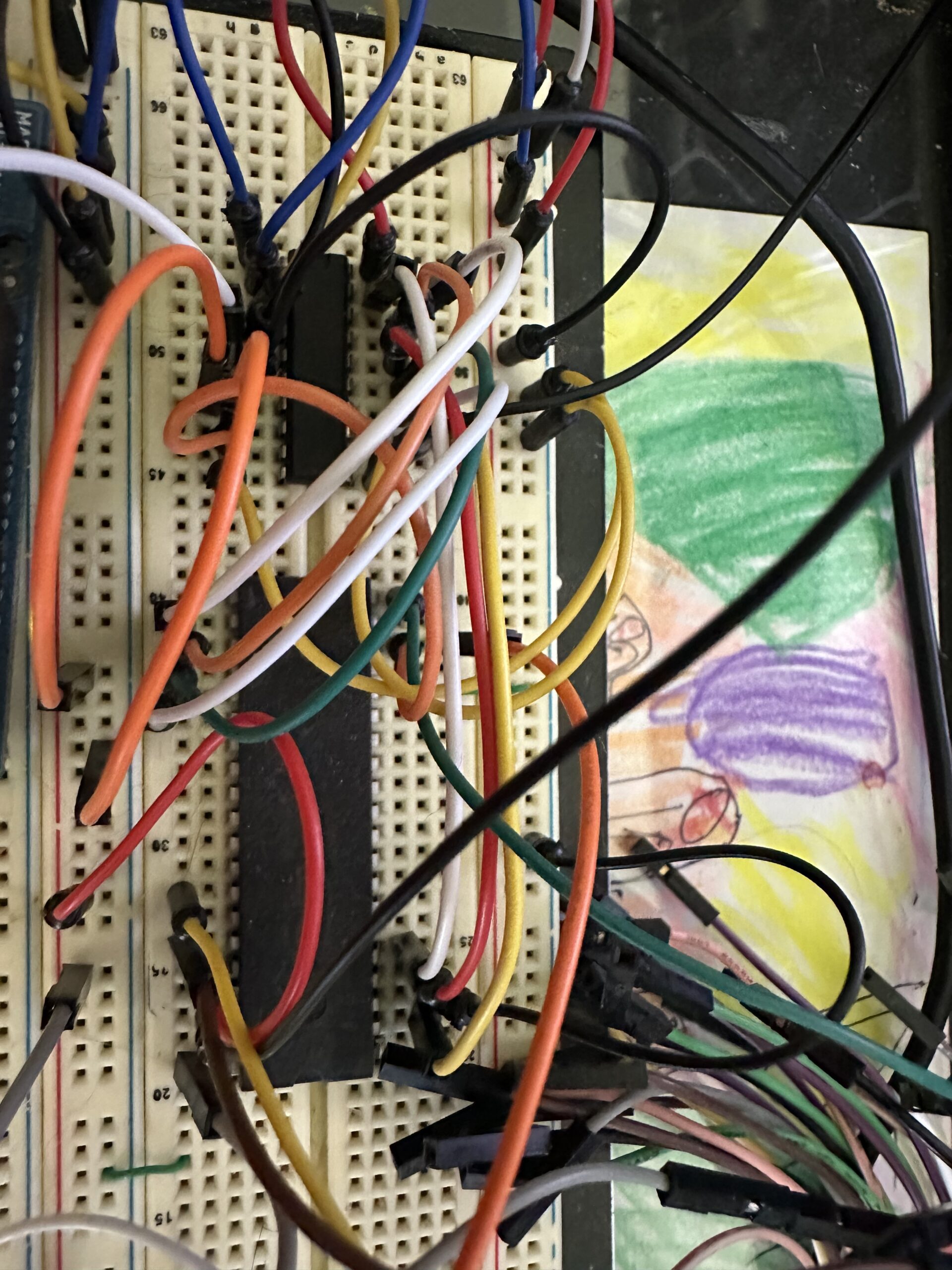
Yes. It’s messy. I had to remove a bunch of unused lines to clean it up because it was getting overcomplicated to connect to the right points.
I’m still using an external power supply – that will be a near term challenge, as I want to use a single 12V supply with +5V and – 5V fixed regulator/converters. Again, I’m still working on the concept of running audio direct without the need to bias it. I may utilize bias voltages for other things, such as phantom microphone voltage, or PTT/COS logic. More to come on that.
so with a little tinkering, and some sample code, it started working exactly as planned! Here’s a video of the code operating. I’/m using X0 – Y0 as my test case. The code is setting this switch ON, waiting 3 seconds, turning it OFF, waiting 3, then turning it ON again. The second ON function then loops into the first, so it ends up being ON (6 sec) OFF (3 sec). The video shows some testing of both the trigger and audio lines to show how it’s all coming together electrically.
I need to do a better schematic of what I have and where it’s going, but this was a big step for an hour on a Saturday morning!
I don’t have video (and it would look the same), but I also changed some of the hard coded address bits to reflect selection of Y1 instead of Y0, and… once I got them in the right order, it worked as expected . (Initially, I was setting the output to 001, but Y4 was turning on and off instead of Y1…. I needed to re-order the data as LSB first, and not MSB first… oops.).
What this DOES prove is that changing the bits around DO, in fact, turn the various switch paths on and off as I wanted, so I made two different advances today.
(edit) I did a little more tinkering – simply alternating between two paths within code. Synchronization was a major issue, since the Arduino needed to boot before the chips, and then HOPE there wasn’t a race condition. To alleviate this, I initially wired both reset pins together, and then to the Arduino, only to find that one was active high, and the other active low. That changed things a bit, so Arduino Pins 7 and 8 are now reset drivers, which toggle appropriately in the setup function.
While I’m on that part… code organization.
- My main variables are defined ahead of all the functions (globals)
- The setup function resets both chips, puts initial values in the bit array that defines the serial stream, and calculates the delays required to define a uniform data rate for the serial stream
- The loop function (currently) sets the output and function (on or off). X0 is hard coded as the input for now.
I plan to add functions for some repetitive tasks (good practice, right?), but right now I’m troubleshooting and learning the processes.
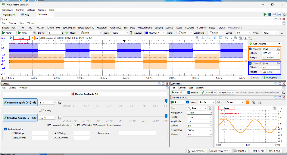
I’m still having a little bit of an issue with inputs turning on or off at the wrong times, which I suspect is due to the strobe line double-pulsing for some reason. This is evident by the first part of the scope shot below. My code is currently written to alternate outputs with a 100 ms delay between toggles. One of my next tasks will be generating a strobe manually from the Arduino and hitting the MT8816 50 ms after I send the serial data.
The next major bit of code is going to be some form of input from the user (buttons and interrupts) to select inputs and outputs as desired. A display will need to be added, too. Then I need to REALLY look into the logic states, so I can get PTT routed, as well. This might be better served by some other logic gates… haven’t figured that out yet. It might also just be a second crosspoint switch. there’s a LOT of logic to figure out, but that’s the easier part now that these two devices are working as desired.
Here’s the block diagram as it stands now (note, some things, such as output enables, are not shown)