Over the past couple weeks, I have been tinkering more with the soundcard interface.
I started using FreePCB (http://www.freepcb.com/) – which is a VERY nice PCB drawing program with gerber file output, and, well, i couldn’t complain about the price! Once I got the “as built” drawing done, I ended up ordering a set of boards from EasyEDA (it was less than 20 bucks for 10 boards!). I also downloaded the demo version of “GerbView”, which will allow some rendering of the gerber files from FreePCB. One other thing I learned about FreePCB is, as long as you enter values and component designations when adding parts, the “report” output will generate a nice parts list.
It was only AFTER I ordered the boards that I started really reviewing the board for possible improvements- I had AUDIO isolation, and discrete switching (CW, PTT) isolation, but serial communications, power, and ground were all still common. This meant I hardly had any isolation at all.
I had already improved the connector pinout to separate serial comms and the audio lines… but how could I add more isolation?
The answer, of course, was more optoisolators… though i thought i was stuck with power and ground breaking the isolation. Then it dawned on me – I could easily use the USB 5VDC to power the pullup resistors on the USB side of the optoisolators, and then use the radio power for the things on the radio side of the isolators. With the power spit, then it was easy to separate ground, as well – since the isolators were using light to bridge that gap.
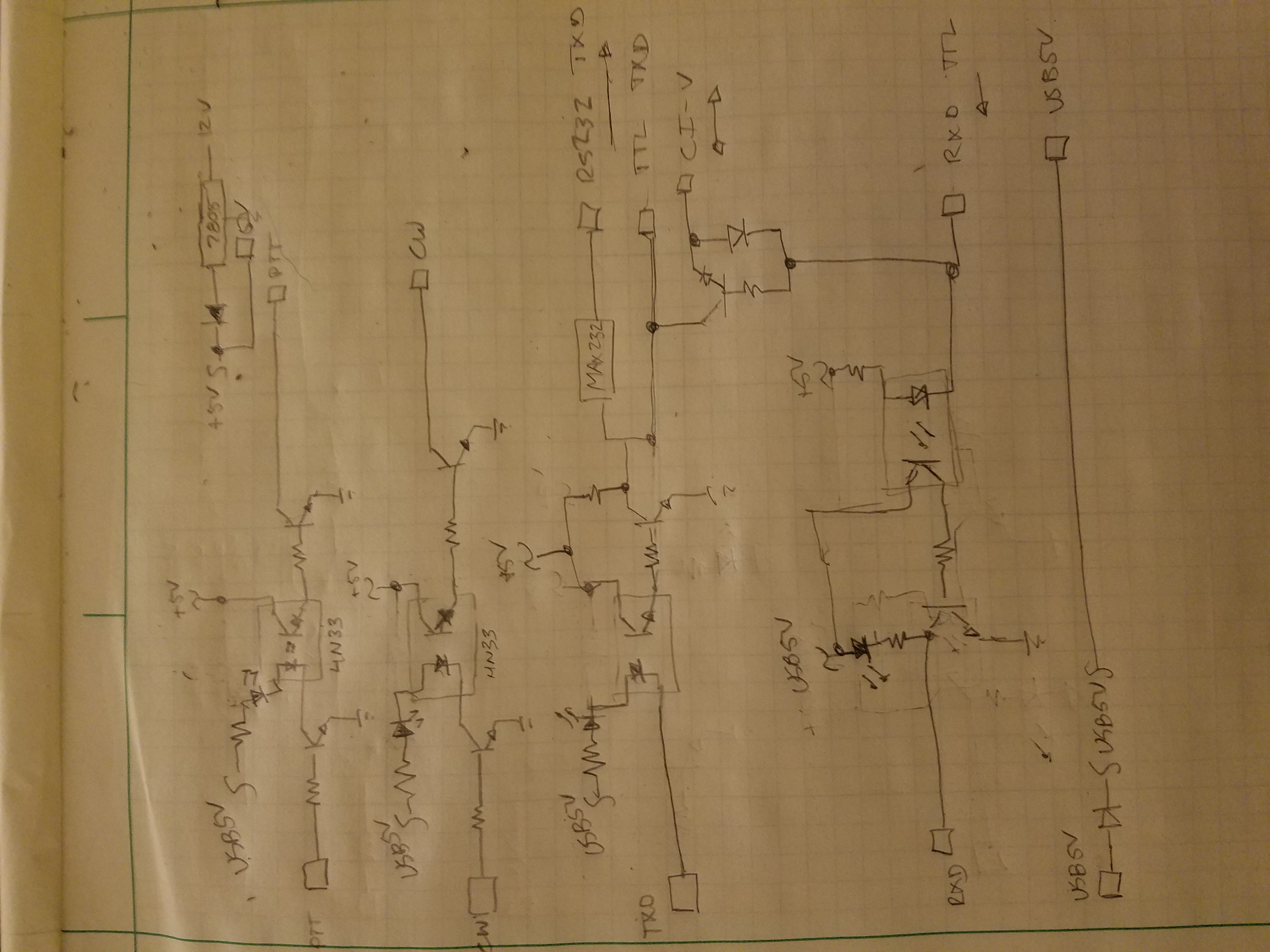
Once I drew the schematic on paper, it was easy to build the PCB the same way as the schematic was laid out – and surprisingly, it opened up a lot of space on the board! Below is the rough hand drawn schematic (note that I forgot to show the Max232 on the radio–> computer TTL line. Click for full size.
I used a quad isolator (LTV847) for everything except the radio–> computer data, which got a dedicated 4N33 chip. This was primarily because of the orientation and trace routing. it would have been possible, just a bit awkward. The rest of the components are simple 10k resistors, 2N3904 NPN transistors, and several diodes. There are 2 isolation transformers and a Max232 converter board – so the circuit provides Isolated RX and TX (TTL), CI-V (single wire TTL comms), and RS232 level comms. It will work with any serial (non-USB) radio, using only an adapter cable.
One thing that I struggled with initially was where the 2N3904 inverter/buffers would be used. Ultimately, the design as shown uses them to invert when necessary, but also to minimize the duty cycle of the LEDs in the optoisolators – so the LEDs are active HIGH, and are off when in an idle state.
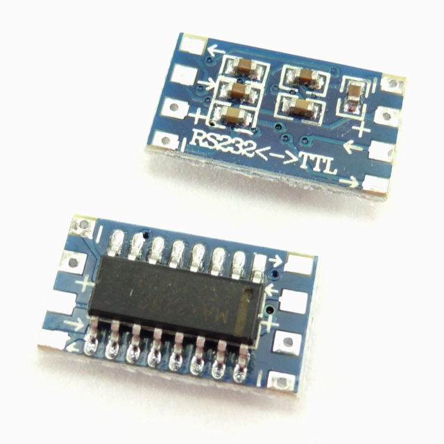
The Max232 module that I used as “U8” on the board is a small module that I’ve used in other projects, found on Ebay for less than $2 each. The intent is to mount pins in the sound card interface (SCI) board, and use the RS232 module like a daughterboard.
Since i had some extra space on the board, I thought that some users may want to springboard off of it for other endeavors, so I routed power (both USB 5V, and regulated radio 5V), as well as ground (USB and radio) near a space where I put a section of perf board between the logic and audio sections. This should be enough to either directly build a circuit, or install a header for a daughter card, depending on the complexity of whatever the user wants to add on.
NOTE: Once i get my first batch of PCBs in, and verify them, I plan on breadboarding the isolated TTL serial comms, then making some minor adjustments to the PCB…. at that point, I’ll post the gerber files in a ZIP file.
First the PCB drawing:
aaannndd… the parts list:
REF VALUE
— ——- —–
C1 10uF
C2 1uF
D1, D2 1N4002
D3 1N4148
D4 – D8 LED
R1 – R14 10k
T1, T2 1:1 audio isolation xfrmer
U1 7805
U2 – U8 2N3904
U9 LTV847
U10 4N33
U20 Max232 board (from Ebay)


