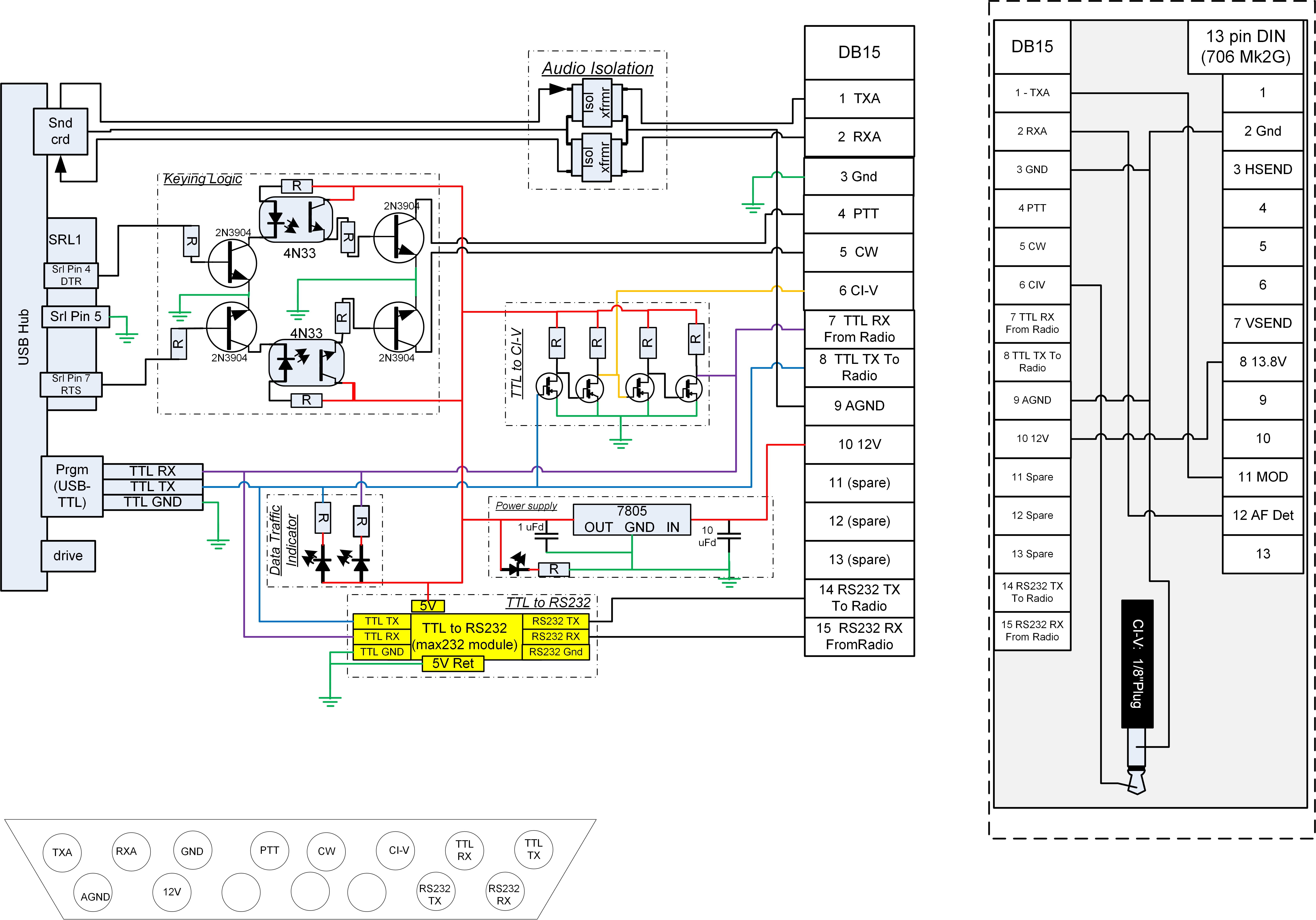
Yesterday I posted the project… now I’ve made some updates…. a few minor things, and one major thing.
First, the minor things-
I made the schematic a bit cleaner, and got it down to a single page. I also cleaned up aa few traces and some other minor formatting things.
I improved the power supply section with some bypass capacitors around the 7805. I’m still contemplating a small zener on the output, but it’s probably not necessary, since I’m expecting the radio to provide operating power.
the one major change I made was to the connector pinout. The original DB15 layout was just simplicity based on the schematic. I rearranged it a bit to better design it for EMI purposes, not that I expect any major EMI issues, but I just decided to use good design practices.
I moved all of the serial communication lines to one side of the connector, and put the sensitive audio lines on the other side. Then, in order to shield things, I placed the audio ground line as close to the two audio lines (pin 9, and 1 & 2, respectively), to limit coupled noise. Additionally, I moved the ground to pin 3, and power to pin 10. This allows the power (12V) and ground to act a bit like guard pins to further provide a low impedance path back to the supply for any noise that might be coupling from other pins. Pins 4 & 5 are reserved for PTT and CW keying, which are logic signals. the CW line is mostly immune to noise, since when it’s operating, the sound card lines won’t be heavily used. Additionally, the PTT line will be grounded when the transmit audio line is in use, so it will, in essence, act like another guard pin.
As I said before, I will have some spare pins – in this case, 11, 12, and 13 will be spares.
It is then apparent that 14 & 15, and 7 & 8 are the serial communication lines, with 6 being the CI-V line.
And without further adieu…. the schematic:
